DSBSC Generation
Achievements:
Definition and modelling of a double sideband suppressed carrier (DSBSC) signal; introduction to the MULTIPLIER, VCO, 60 kHz LPF, and TUNEABLE LPF modules; spectrum estimation; multipliers and modulators.
Prerequisites:
Completion of the experiment entitled ‘Modelling an equation’ in this Volume.
PREPARATION
This experiment will be your introduction to the MULTIPLIER and the double sideband suppressed carrier signal, or DSBSC. This modulated signal was probably not the first to appear in an historical context, but it is the easiest to generate.
You will learn that all of these modulated signals are derived from low frequency signals, or ‘messages’. They reside in the frequency spectrum at some higher frequency, being placed there by being multiplied with a higher frequency signal, usually called ‘the carrier’
Definition of a DSBSC
Consider two sinusoids, or cosinusoids, cosμt and coswt. A double sideband suppressed carrier signal, or DSBSC, is defined as their product, namely:
DSBSC = E.cosμt . cosωt Eq.1
Generally, and in the context of this experiment, it is understood that::
ω >> μ Eq. 2
Equation (3) can be expanded to give:
cosμt . cosωt = (E/2) cos(ω - μ)t + (E/2) cos(ω + μ)t Eq. 3
Equation 3 shows that the product is represented by two new signals, one on the sum frequency (ω + μ), and one on the difference frequency (ω - μ) - see Figure 1.
Remembering the inequality of eqn. (2) the two new components are located close to the frequency ω rad/s, one just below, and the other just above it. These are referred to as the lower and upper sidebands respectively.
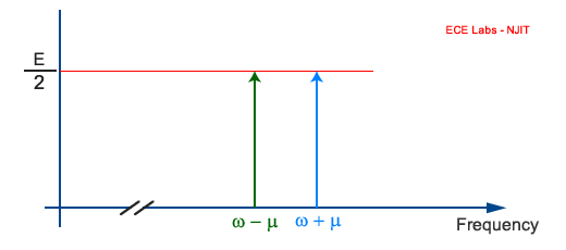
Figure 1: Spectral components
These two components were derived from a ‘carrier’ term on ω rad/s, and a message on μ rad/s. Because there is no term at carrier frequency in the product signal it is described as a double sideband suppressed carrier (DSBSC) signal.
The term ‘carrier’ comes from the context of ‘double sideband amplitude modulation’ (commonly abbreviated to just AM).
AM is introduced in a later experiment (although, historically, AM preceded DSBSC).
The time domain appearance of a DSBSC (eqn. 1) in a text book is generally as shown in Figure 2.
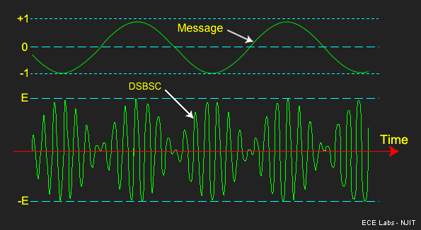
Figure 2: Eqn.(1) - a DSBSC - seen in the time domain
Notice the waveform of the DSBSC in Figure 2, especially near the times when the message amplitude is zero. The fine detail differs from period to period of the message. This is because the ratio of the two frequencies μ and ω has been made non-integral.
Although the message and the carrier are periodic waveforms (sinusoids), the DSBSC itself need not necessarily be periodic.
block diagram
A block diagram, showing how eqn. (1) could be modelled with hardware, is shown in Figure 3 below.
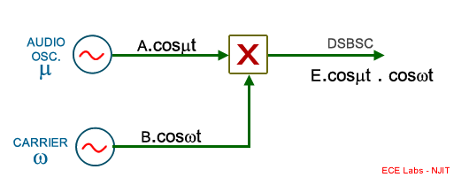
Figure 3: Block diagram to generate eqn. (1) with hardware.
Viewing envelopes
This is the first experiment dealing with a narrow band signal. Nearly all modulated signals in communications are narrow band. The definition of 'narrow band' has already been discussed in the chapter Introduction to Modelling with TIMS.
You will have seen pictures of DSB or DSBSC signals (and amplitude modulation - AM) in your text book, and probably have a good idea of what is meant by their envelopes. You will only be able to reproduce the text book figures if the oscilloscope is set appropriately - especially with regard to the method of its synchronization. Any other methods of setting up will still be displaying the same signal, but not in the familiar form shown in text books. How is the 'correct method' of synchronization defined?
With narrow-band signals, and particularly of the type to be examined in this and the modulation experiments to follow, the following steps are recommended:
- Use a single tone for the message, say 1 kHz.
- Synchronize the oscilloscope to the message generator, which is of fixed amplitude, using the 'ext trig.' facility.
- Set the sweep speed so as to display one or two periods of this message on one channel of the oscilloscope.
- Display the modulated signal on another channel of the oscilloscope.
With the recommended scheme the envelope will be stationary on the screen. In all but the most special cases the actual modulated waveform itself will not be stationary - since successive sweeps will show it in slightly different positions. So the display within the envelope - the modulated signal - will be 'filled in', as in Figure 4, rather than showing the detail of Figure 2
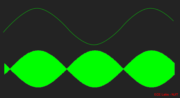
Figure 4: Typical display of a DSBSC, with the message from which it was derived,
as seen on an oscilloscope. Compare with Figure 2
multi-tone message
The DSBSC has been defined in eqn. (1), with the message identified as the low frequency term. Thus:
message = cosμt Eq. 4
For the case of a multi-tone message, m(t), where:
 Eq. 5
Eq. 5
then the corresponding DSBSC signal consists of a band of frequencies below ω, and a band of frequencies above ω. Each of these bands is of width equal to the bandwidth of m(t).
The individual spectral components in these sidebands are often called sidefrequencies.
If the frequency of each term in the expansion is expressed in terms of its difference from ω, and the terms are grouped in pairs of sum and difference frequencies, then there will be ‘n’ terms of the form of the right hand side of eqn. (3).
Note it is assumed here that there is no DC term in m(t). The presence of a DC term in m(t) will result in a term at ω in the DSB signal; that is, a term at ‘carrier’ frequency. It will no longer be a double sideband suppressed carrier signal. A special case of a DSB with a significant term at carrier frequency is an amplitude modulated signal, which will be examined in an experiment to follow.
A more general definition still, of a DSBSC, would be:
DSBSC = E.m(t).cosωt Eq. 6
where m(t) is any (low frequency) message. By convention m(t) is generally understood to have a peak amplitude of unity (and typically no DC component).
Linear Modulation
The DSBSC is a member of a class known as linear modulated signals. Here the spectrum of the modulated signal, when the message has two or more components, is the sum of the spectral components which each message component would have produced if present alone.
For the case of non-linear modulated signals, on the other hand, this linear addition does not take place. In these cases the whole is more than the sum of the parts. A frequency modulated (FM) signal is an example. These signals are first examined in the chapter entitled Analysis of the FM spectrum, within Volume A2 - Further & Advanced Analog Experiments, and subsequent experiments of that Volume.
Spectrum analysis
In the experiment entitled Spectrum analysis - the WAVE ANALYSER, within Volume A2 - Further & Advanced Analog Experiments, you will model a WAVE ANALYSER. As part of that experiment you will re-examine the DSBSC spectrum, paying particular attention to its spectrum.
EXPERIMENT
The Multiplier
This is your introduction to the MULTIPLIER module.
Please read the section in the chapter of this Volume entitled Introduction to modelling with TIMS headed multipliers and modulators. Particularly note the comments on DC off-sets.
Preparing the model
Figure 3 shows a block diagram of a system suitable for generating DSBSC derived from a single tone message.
Figure 5 shows how to model this block diagram with TIMS.
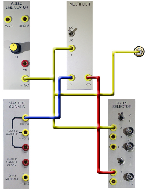
Figure 5: Pictorial of block diagram of Figure 3
The signal A.cosμt, of fixed amplitude A, from the AUDIO OSCILLATOR, represents the single tone message. A signal of fixed amplitude from this oscillator is used to synchronize the oscilloscope.
The signal B.coswt, of fixed amplitude B and frequency exactly 100 kHz, comes from the MASTER SIGNALS panel. This is the TIMS high frequency, or radio, signal. Text books will refer to it as the 'carrier signal'.
The amplitudes A and B are nominally equal, being from TIMS signal sources. They are suitable as inputs to the MULTIPLIER, being at the TIMS ANALOG REFERENCE LEVEL. The output from the MULTIPLIER will also be, by design of the internal circuitry, at this nominal level. There is no need for any amplitude adjustment. It is a very simple model.
T1 Patch up the arrangement of Figure 5.
T2 Use the FREQUENCY COUNTER to set the AUDIO OSCILLATOR to about 1 kHz
Figure 2 shows the way most text books would illustrate a DSBSC signal of this type. But the display you have in front of you is more likely to be similar to that of Figure 4.
Signal amplitude.
T3 Measure and record the amplitudes A and B of the message and carrier signals at the inputs to the MULTIPLIER.
The output of this arrangement is a DSBSC signal, and is given by:
DSBSC = k A.cosμt B.cosωt Eq. 7
The peak-to-peak amplitude of the display is:
peak-to-peak = 2 k A B volts Eq. 8
Here 'k' is a scaling factor, a property of the MULTIPLIER. One of the purposes of this experiment is to determine the magnitude of this parameter.
Now:
T4 measure the peak-to-peak amplitude of the DSBSC
Since you have measured both A and B already, you have now obtained the magnitude of the MULTIPLIER scale factor 'k'; thus:
k = (dsbsc peak-to-peak) / (2 A B) Eq. 9
Note that 'k' is not a dimensionless quantity.
Fine detail in the time domain
The oscilloscope display will not in general show the fine detail inside the DSBSC, yet many textbooks will do so, as in Figure 2. Figure 2 would be displayed by a single sweep across the screen. The normal laboratory oscilloscope cannot retain and display the picture from a single sweep. Subsequent sweeps will all be slightly different, and will not coincide when superimposed.
To make consecutive sweeps identical, and thus to display the DSBSC as depicted in Figure 2, it is necessary that ‘μ’ be a sub-multiple of ‘ω’. This special condition can be arranged with TIMS by choosing the '2 kHz MESSAGE' sinusoid from the fixed MASTER SIGNALS module. The frequency of this signal is actually 100/48 kHz (approximately 2.08 kHz), an exact sub-multiple of the carrier frequency. Under these special conditions the fine detail of the DSBSC can be observed.
T5 Obtain a display of the DSBSC similar to that of Figure 2. A sweep speed of, say, 50μs/cm is a good starting point.
Overload
When designing an analog system signal overload must be avoided at all times. Analog circuits are expected to operate in a linear manner, in order to reduce the chance of the generation of new frequencies. This would signify non-linear operation.
A multiplier is intended to generate new frequencies. In this sense it is a nonlinear device. Yet it should only produce those new frequencies which are wanted - any other frequencies are deemed unwanted.
A quick test for unintended (non-linear) operation is to use it to generate a signal with a known shape -a DSBSC signal is just such a signal. Presumably so far your MULTIPLIER module has been behaving ‘linearly’.
T6 Insert a BUFFER AMPLIFIER in one or other of the paths to the MULTIPLIER, and increase the input amplitude of this signal until overload occurs. Sketch and describe what you see.
Bandwidth
Equation (3) shows that the DSBSC signal consists of two components in the frequency domain, spaced above and below ω by μ rad/s.
With the TIMS BASIC SET of modules, and a DSBSC based on a 100 kHz carrier, you can make an indirect check on the truth of this statement. Attempting to pass the DSBSC through a 60 kHz LOWPASS FILTER will result in no output, evidence that the statement has some truth in it - all components must be above 60 kHz.
A convincing proof can be made with the 100 kHz CHANNEL FILTERS module 5. Passage through any of these filters will result in no change to the display (see alternative spectrum check later in this experiment).
Using only the resources of the TIMS BASIC SET of modules a convincing proof is available if the carrier frequency is changed to, say, 10 kHz. This signal is available from the analog output of the VCO, and the test setup is illustrated in Figure 6 below. Lowering the carrier frequency puts the DSBSC in the range of the TUNEABLE LPF.
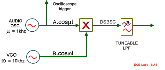
Figure 6: Checking the spectrum of a DSBSC signal
T7 Read about the VCO module in the TIMS User Manual. Before plugging the VCO in to the TIMS SYSTEM UNIT set the on-board switch to VCO. Set the front panel frequency range selection switch to ‘LO’.
T8 Read about the TUNEABLE LPF in the TIMS User Manual and the Appendix A to this text.
T9 Set up an arrangement to check out the TUNEABLE LPF module. Use the VCO as a source of sinewave input signal. Synchronize the oscilloscope to this signal. Observe input to, and output from, the TUNEABLE LPF.
T10 Set the front panel GAIN control of the TUNEABLE LPF so that the gain through the filter is unity.
T11 Confirm the relationship between VCO frequency and filter cutoff frequency (refer to the TIMS User Manual for full details, or the Appendix to this Experiment for abridged details).
T12 Set up the arrangement of Figure 6. Your model should look something like that of Figure 7, where the arrangement is shown modelled by TIMS.
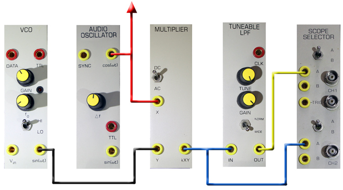
Figure 7: TIMS model of Figure 6
T13 Adjust the VCO frequency to about 10 kHz
T14 Set the AUDIO OSCILLATOR to about 1 kHz.
T15 Confirm that the output from the MULTIPLIER looks like Figures 2 and/or 4. Analysis predicts that the DSBSC is centred on 10 kHz, with lower and upper sidefrequencies at 9.0 kHz and 11.0 kHz respectively. Both sidefrequencies should fit well within the passband of the TUNEABLE LPF, when it is tuned to its widest passband, and so the shape of the DSBSC should not be altered.
T16 Set the front panel toggle switch on the TUNEABLE LPF to WIDE, and the front panel TUNE knob fully clockwise. This should put the passband edge above 10 kHz. The passband edge (sometimes called the ‘corner frequency’) of the filter can be determined by connecting the output from the TTL CLK socket to the FREQUENCY COUNTER. It is given by dividing the counter readout by 360 (in the ‘NORMAL’ mode the dividing factor is 880).
T17 Note that the passband GAIN of the TUNEABLE LPF is adjustable from the front panel. Adjust it until the output has a similar amplitude to the DSBSC from the MULTIPLIER (it will have the same shape). Record the width of the passband of the TUNEABLE LPF under these conditions.
Assuming the last Task was performed successfully this confirms that the DSBSC lies below the passband edge of the TUNEABLE LPF at its widest. You will now use the TUNEABLE LPF to determine the sideband locations. That this should be possible is confirmed by Figure 8 below.
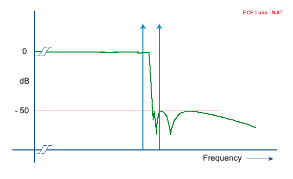
Figure 8: the amplitude response of the TUNEABLE LPF superimposed on the DSBSC spectrum.
Figure 8 shows the amplitude response of the TUNEABLE LPF superimposed on the DSBSC, when based on a 1 kHz message. The drawing is approximately to scale. It is clear that, with the filter tuned as shown (passband edge just above the lower sidefrequency), it is possible to attenuate the upper sideband by 50 dB and retain the lower sideband effectively unchanged.
T18 Make a sketch to explain the meaning of the transition bandwidth of a lowpass filter. You should measure the transition bandwidth of your TUNEABLE LPF, or instead accept the value given in Appendix A to this text.
T19 Lower the filter passband edge until there is a just-noticeable change to the DSBSC output. Record the filter passband edge as fA. You have located the upper edge of the DSBSC at (w + μ) rad/s.
T20 Lower the filter passband edge further until there is only a sinewave output. You have isolated the component on (ω - μ) rad/s. Lower the filter passband edge still further until the amplitude of this sinewave just starts to reduce. Record the filter passband edge as fB.
T21 Again lower the filter passband edge, just enough so that there is no significant output. Record the filter passband edge as fC.
T22 From a knowledge of the filter transition band ratio, and the measurements fA and fB , estimate the location of the two sidebands and compare with expectations. You could use fC as a cross-check.
Alternative spectrum check
If you have a 100kHz CHANNEL FILTERS module, or from a SPEECH module, then, knowing the filter bandwidth, it can be used to verify the theoretical estimate of the DSBSC bandwidth.
speech as the message
If you have speech available at TRUNKS you might like to observe the appearance of the DSBSC signal in the time domain.
Figure 9 is a snap-shot of what you might see.
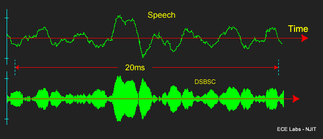
Figure 9: speech derived DSBSC
TUTORIAL QUESTIONS
Q1 In TIMS the parameter 'k' has been set so that the product of two sinewaves, each at the TIMS ANALOG REFERENCE LEVEL, will give a MULTIPLIER peak-to-peak output amplitude also at the TIMS ANALOG REFERENCE LEVEL. Knowing this, predict the expected magnitude of 'k'
Q2 How would you answer the question 'what is the frequency of the signal y(t) = E.cosμt.cosωt'?
Q3 What would the FREQUENCY COUNTER read if connected to the signal y(t) = E.cosμt.cosωt?
Q4 Is a DSBSC signal periodic?
Q5 Carry out the trigonometry to obtain the spectrum of a DSBSC signal when the message consists of three tones, namely:
message = A1.cosμ1t + A2.cosμ2t + A3 cosμ3t
Show that it is the linear sum of three DSBSC, one for each of the individual message components.
Q6 The DSBSC definition of eqn. (1) carried the understanding that the message frequency μ should be very much less than the carrier frequency ω. Why was this? Was it strictly necessary? You will have an opportunity to consider this in more detail in the experiment entitled Envelopes (within Volume A2 - Further & Advanced Analog Experiments).