Lab 5: Phase Modulation and Constellations.
Achievements:
Generation of binary phase shift keyed (BPSK) signal; bandlimiting; synchronous demodulation - phase ambiguities.
Prerequisites:
Familiarity with the DECISION MAKER, LINECODE ENCODER and LINE-CODE DECODER modules is assumed.
Extra Modules:
Read the prelab and make the list of the extra modules needed for this lab based on your reading.
Prelab
PART 1: Generation of BPSK
Consider a sinusoidal carrier. If it is modulated by a bi-polar bit stream according to the scheme illustrated in Figure 1 below, its polarity will be reversed every time the bit stream changes polarity. This, for a sinewave, is equivalent to a phase reversal (shift). The multiplier output is a BPSK signal.
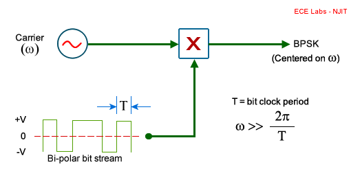
Figure 1: Generation of BPSK
The information about the bit stream is contained in the changes of phase of the transmitted signal. A synchronous demodulator would be sensitive to these phase reversals. The appearance of a BPSK signal in the time domain is shown in Figure 2 (lower trace). The upper trace is the binary message sequence.
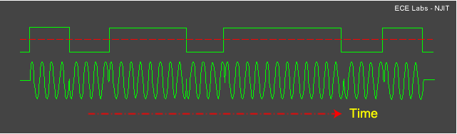
Figure 2: A BPSK signal in the time domain.
There is something special about the waveform of Figure 2. The wave shape is 'symmetrical' at each phase transition. This is because the bit rate is a submultiple of the carrier frequency ω/(2π). In addition, the message transitions have been timed to occur at a zero-crossing of the carrier.
Whilst this is referred to as 'special', it is not uncommon in practice. It offers the advantage of simplifying the bit clock recovery from a received signal. Once the carrier has been acquired then the bit clock can be derived by division.
But what does it do to the bandwidth? See Tutorial Question Q4.
Bandlimiting
The basic BPSK generated by the simplified arrangement illustrated in Figure 1 will have a bandwidth in excess of that considered acceptable for efficient communications.
If you can calculate the spectrum of the binary sequence then you know the bandwidth of the BPSK itself. The BPSK signal is a linearly modulated DSB, and so it has a bandwidth twice that of the baseband data signal from which it is derived (this assumes ω > 2B).
In practice there would need to be some form of bandwidth control.
Bandlimiting can be performed either at baseband or at carrier frequency. It will be performed at baseband in this experiment.
BPSK demodulation
Demodulation of a BPSK signal can be considered a two-stage process.
- Translation back to baseband, with recovery of the bandlimited message waveform
- Regeneration from the bandlimited waveform back to the binary message bit stream.
Translation back to baseband requires a local, synchronized carrier.
Stage 1
Translation back to baseband is achieved with a synchronous demodulator, as shown in Figure 3 below.
This requires a local synchronous carrier. In this experiment a stolen carrier will be used.
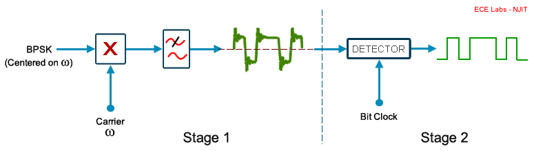
Figure 3: Synchronous demodulation of BPSK
Stage 2
The translation process does not reproduce the original binary sequence, but a bandlimited version of it.
The original binary sequence can be regenerated with a detector. This requires information regarding the bit clock rate. If the bit rate is a sub-multiple of the carrier frequency then bit clock regeneration is simplified.
In TIMS the DECISION MAKER module can be used for the regenerator, and in this experiment the bit clock will be a sub-multiple of the carrier.
Phase ambiguity
You will see in the experiment that the sign of the phase of the demodulator carrier is important.
Phase ambiguity is a problem in the demodulation of a BPSK signal.
There are techniques available to overcome this. One such sends a training sequence, of known format, to enable the receiver to select the desired phase, following which the training sequence is replaced by the normal data (until synchronism is lost!).
An alternative technique is to use differential encoding. This will be demonstrated in this experiment by selecting a different code from the LINE-CODE ENCODER.
EXPERIMENT
The BPSK generator
The BPSK generator of Figure 1 is shown in expanded form in Figure 4, and modelled in Figure 5
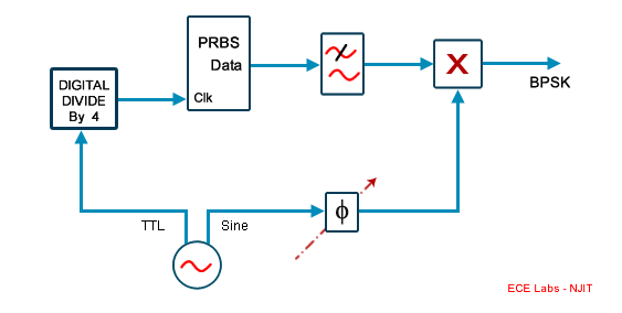
Figure 4: Block diagram of BPSK generator to be modelled
Note that the carrier will be four times the bit clock rate.
The lowpass filter is included as a band limiter if required. Alternatively a bandpass filter could have been inserted at the output of the generator. Being a linear system, the effect would be the same.
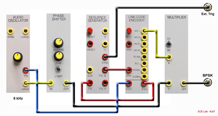
Figure 5: Model of the BPSK generator
The AUDIO OSCILLATOR supplies a TTL signal for the bit clock digital DIVIDEBY- FOUR sub-system in the LINE-CODE ENCODER, and a sinusoidal signal for the carrier.
The PHASE SHIFTER (set to the LO range with the on-board switch SW1) allows relative phase shifts. Watch the phase transitions in the BPSK output signal as this phase is altered. This PHASE SHIFTER can be considered optional.
The digital DIVIDE-BY-FOUR sub-system within the LINE-CODE ENCODER is used for deriving the bit clock as a sub-multiple of the BPSK carrier. Because the DECISION MAKER, used in the receiver, needs to operate in the range about 2 to 4 kHz, the BPSK carrier will be in the range about 8 to 16 kHz.
The NRZ-L code is selected from LINE-CODE ENCODER.
Viewing of the phase reversals of the carrier is simplified because the carrier and binary clock frequencies are harmonically related.
T1 Patch up the modulator of Figure 5; acquaint yourself with a BPSK signal. Examine the transitions as the phase between bit clock and carrier is altered. Vary the phase shift and examine its effect on the spectrum. Can you explain this? Vary the bandwidth of the PRBS with the TUNEABLE LPF. Notice the envelope.
BPSK demodulator
Figure 3 shows a synchronous demodulator for a BPSK signal in block diagram form. This has been modelled in Figure 6 below. In the first part of the experiment the carrier and bit clocks will be stolen.
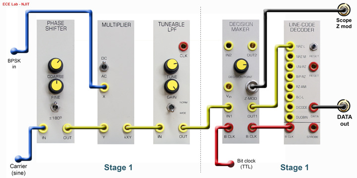
Figure 6: The BPSK demodulator
The phase of the carrier is adjustable with the PHASE SHIFTER for maximum output from the lowpass filter. Phase reversals of 180o can be introduced with the front panel toggle switch.
Select the NRZ-L input to the LINE-CODE DECODER. The LINE-CODE ENCODER and LINE-CODE DECODER modules are not essential in terms of the coding they introduce (since a bi-polar sequence is already available from the SEQUENCE GENERATOR) but they are useful in that they contain the DIVIDE-BYFOUR sub-systems, which are used to derive the sub-multiple bit clock.
The LPF following the demodulator multiplier is there to remove the components at double the carrier frequency. Its bandwidth can be set to about 12 kHz; although, for maximum signal-to-noise ratio (if measuring bit error rates, for example), something lower would probably be preferred.
Measurements
The BPSK will have been bandlimited by the lowpass filter in the transmitter, and so the received waveform is no longer rectangular in shape. But you can observe that the demodulator filter output is related to the transmitted sequence (the NRZ-L code introduces only a level shift and amplitude scale).
The DECISION MAKER will regenerate the original TTL sequence waveform.
Notice the effect upon the recovered sequence when the carrier phase is reversed at the demodulator.
The following Tasks are a reminder of what you might investigate.
T2 Patch up the demodulator of Figure 6. The received signal will have come from the transmitter of Figure 5. Observe the output from the TUNEABLE LPF, and confirm its appearance with respect to that transmitted. If the sequence is inverted then toggle the front panel 1800 switch of the receiver PHASE CHANGER.
T3 Set the on-board switch SW1 of the DECISION MAKER to accept NRZ-L coding. Use the gain control of the TUNEABLE LPF to set the input at about the TIMS ANALOG REFERENCE LEVEL of ± 2 volt peak. Adjust the decision point. Check the output.
T4 Observe the TTL output from the LINE-CODE DECODER. Confirm that the phase of the receiver carrier (for the NRZ-L line code) is still important.
T5 Investigate a change of bandwidth of the transmitted signal. Notice that, as the bandwidth is changed, the amplitude of the demodulated sequence at the DECISION MAKER input will change. This you might expect; but, under certain conditions, it can increase as the bandwidth is decreased ! How could this be? See Tutorial Question Q6.
TUTORIAL QUESTIONS
Q1 Do you think BPSK is an analog signal? Any comments?
Q2 In the model of Figure 5, is it necessary that the MULTIPLIER be switched to DC, as shown?
Q3 You observed the shape of the phase transitions as the PHASE SHIFTER of Figure 5 was changed. Would this influence the spectrum of the BPSK signal?
Q4 Does making the bit rate a sub-multiple of the carrier frequency have any influence on the spectrum of the BPSK signal?
Q5 What is the purpose of the lowpass filter in the BPSK demodulator model ? What determines its bandwidth?
Q6 The amplitude of the signal at the DECISION MAKER input can decrease as the bandwidth of the transmitter is widened (or vice versa). At first glance this seems unusual? Explain.
Q7 The PHASE SHIFTER in the demodulator of Figure 6 was adjusted for maximum output. What phase was it optimizing, and what was the magnitude of this phase? Could you measure it?
Part 2: QPSK and m-ary PSK
An introduction to the M-LEVEL ENCODER and M-LEVEL DECODER modules; the signal constellations of m- PSK. Decoding.
Prerequisites:
A theoretical introduction to m-PSK.
PREPARATION
In these applications the modulator requires a pair of multi-level analog signals derived from a single serial binary data stream.
To derive these two signals TIMS uses the M-LEVEL ENCODER module.
At the demodulator a complementary module, the M-LEVEL DECODER, is used.
These two modules will be examined in this experiment, independently of the quadrature amplitude modulator and demodulator with which they will later be associated.
Their purpose will be better understood if you are first reminded of their role in a quadrature modulator and quadrature demodulator.
Terminology
The two outputs from the M-LEVEL ENCODER are referred to as the I and Q signals. Here the ‘I’ and the ‘Q’ refer to inphase and quadrature, which describe the phase of the carriers of the DSBSC modulators to which they are connected.
The upper case ‘M’ in the module names is intended to imply that the I and Q output signals are ‘Multi-level’. This is not a common usage of the symbol ‘M’.
It is not the same as the lower case ‘m’ used here in the abbreviations m-PSK and m-QAM. The ‘m’ in these names refers specifically to the number of points in the constellation diagram (to be defined later), and is derived from the number of bits, L, in the frame (defined later), determined by the encoding process.
You will see that:
m = 2 L
The quadrature modulator
As a reminder, a block diagram of a quadrature modulator is shown in Figure 1. This configuration is common to many communications systems.
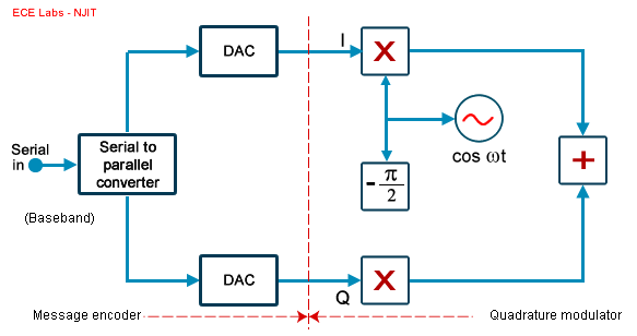
Figure 1: An m-QAM modulator.
Encoding
To generate the two multi-level analog signals mentioned above the input serial binary data stream is segmented into frames (or binary words) of L bits each, in a serial-to-parallel converter.
For a particular choice of L there will be m = 2L unique words.
From each of these words is generated a unique pair of analog voltages, one of which goes to the I-path, and the other to the Q-path, of the quadrature modulator.
A typical arrangement is illustrated in block diagram form in Figure 1 above.
No bandlimiting is shown in Figure 1, but in practice this would be introduced either at the input to each multiplier (possibly in the form of a pulse shaping filter), or at the output of the adder, or both.
Demodulation
A quadrature demodulator is illustrated in Figure 2. Remember the input signal is a pair of DSBSC, added in phase quadrature. It is the purpose of the demodulator to recover their individual messages, which are presented to the two inputs of the decoder. If the DSBSC phasing at the transmitter is ideally in quadrature, then the single phase adjustment shown is sufficient to separate the messages of the two signals.
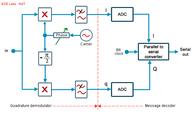
Figure 2: A`n m-QAM demodulator
Decoding
Each arm of the decoder is presented with a bandlimited analog waveform.
The decoder has a bit clock input (stolen in the experiment, else derived from the incoming signal in practice) and knows beforehand the number of bit periods (L) in a frame.
Each waveform is sampled once per frame, and a decision made as to which of the possible levels it represents. This will give a unique pair of levels, which represents a binary word of L bits. This decoded word is output as a serial binary data stream.
Constellations
Associated with these signals are phasor diagrams, and signal constellation diagrams.
The phasor diagram is one of the many ways in which some of the properties of these bandpass signals can be illustrated.
Each phasor represents the output signal during each of the frames.
The signal constellation diagram shows the location of the tips of these phasors on the complex plane.
It is displayed when the two baseband multi-level signals I and Q are connected to the X and Y inputs of an oscilloscope (in X-Y mode).
These signals can come from the encoder output, or from the decoder input. The first of these shows the constellation under ideal conditions. The second shows the constellation after the signal has passed through the channel.
In the second case the display can be used to reveal much about the impairments suffered by the signal.
Much research has gone into the optimum location of these points in the constellation, in order to obtain the most desirable properties - or combination of properties.
Naming conventions
Typically the signal constellation is a symmetrical display. Depending upon the disposition of the points in the display so the resulting modulated signal has different properties, and is given different names.
For example, the points could be in a circle - such as in m-PSK, or in a square grid, as in m-QAM. These constellations are illustrated below in Figure 3, for the case m = 8. In these cases the binary serial data stream has been encoded using frames of three bits.
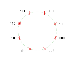
8-PSK
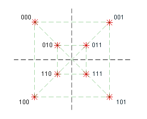
8-QAM
Figure 3: Constellation diagrams
The three-bit words located near each point are the bits in the frame with which each point is associated.
More information
For further theoretical detail on these signals and systems see your Text book.
You can find more technical information about the M-LEVEL ENCODER and MLEVEL DECODER modules in the Advanced Modules User Manual.
EXPERIMENT
M-LEVEL ENCODER module
The arrangement to be examined first is that designated as the ‘message encoder’ of Figure 1, together with a message source. These are modelled in Figure 4 below.
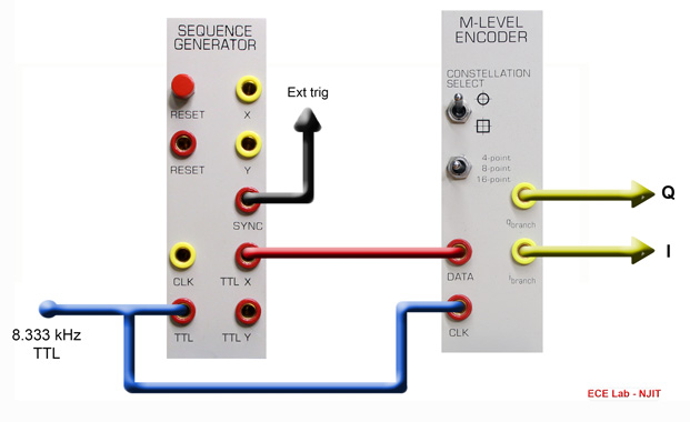
Figure 4: The encoder with 4-QAM selected
As shown, the input is a serial binary data stream from a SEQUENCE GENERATOR. The multilevel I and Q output signals would go to the quadrature modulator (typically preceded by identical lowpass filters).
T1 Obtain an M-LEVEL ENCODER module. Before plugging it in ensure that the on-board jumper J3 is in the ‘NORMAL’ position. The purpose of each of the sockets and controls on the front panel should be selfexplanatory.
T2 Patch up the arrangement of Figure 4. Start with a short sequence from the SEQUENCE GENERATOR (both toggles of the on-board switch SW2 should be UP), and select 4-QPSK from the M-LEVEL ENCODER.
Constellations
T3 Predict the appearance of the constellation diagram, and then display it on the oscilloscope (the I and Q signals connect to the X and Y inputs of the oscilloscope to represent the complex plane with the imaginary axis vertical).
Coding schemes
You will now deduce the coding scheme of the 4-QPSK signal. This can be done by examining simultaneously the input data and each one of the I and Q output signals in turn. The encoder will have arbitrarily selected the frame start point in the incoming serial binary data stream. Each frame will contain two data bits (for the 4-QPSK case).
The first requirement, when looking at the input serial binary data stream, is that you must decide where a frame starts. This would be easy if there was not a processing delay (of several clock periods at least) between the end of the frame and the start of the encoded I or Q output.
Some heuristics will be necessary.
Remember, you do know the frame length.
T4 Display the input serial stream and the I output signal. Deduce the coding scheme used to map the input data to the output. Repeat for the Q output. Record the magnitude of the delay between the frame and the corresponding encoded output (as a function of the input data clock period). There will not necessarily be the same delay for other constellations.
As time permits the previous two Tasks could be repeated for other constellations. Note that, for larger constellations, it would be necessary to increase the sequence length. Explain.
T5 Examine the constellations of each of the other signals available from the MLEVEL ENCODER. Notice the result of using a short sequence.
Eye patterns
T6 Display the eye patterns for all of the possible signals from the encoder. Note and record the number and magnitude of the voltage levels involved. Remember, to view all possible levels, long sequences are necessary. Explain.
If you previously displayed the eye patterns before first bandlimiting the signals, so be it. But more representative patterns result if bandlimiting is first introduced.
T7 View the eye patterns of the previous Task with bandlimiting, if not already done so.
Having acquainted yourself with the encoder properties, those of the decoder may now be examined.
M-LEVEL DECODER module
The decoder would normally be provided with the inphase and quadrature outputs from a quadrature amplitude demodulator. These would be noisy, bandlimited baseband signals. Each must be ‘cleaned up’ and their absolute levels adjusted so as to be suitable for analog-to-digital decoding.
The ‘cleaning up’ and decoding is performed by the M-LEVEL DECODER module.
Figure 5 is a model of the m-QPSK decoder shown in block diagram form in Figure 2. Its operation will now be examined.
The I and Q signals from the encoder are shown bandlimited by a pair of lowpass filters, the better to simulate the output of a typical quadrature demodulator.
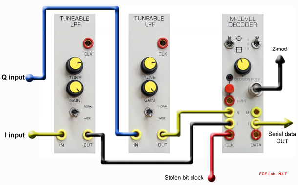
Figure 5: Decoder - switched for 4-QAM
Obtain an M-LEVEL DECODER module. Before plugging it in ensure that the onboard RANGE jumper is in the 'HI' position (suits a clock between 4 kHz and 10 kHz). The purpose of each of the sockets and controls on the front panel should be self-explanatory, except perhaps for those associated with the HUNT facility. This will be introduced below.
T8 Patch up the decoding model of Figure 5. Set the front panel switches to decode 4-QAM. Initially, at least, set both the TUNEABLE LPF modules to maximum bandwidth.
Eye diagrams
The decision point can be moved with the front panel DECISION POINT control. The amount of movement is a little over one bit period. The point can be moved in coarse (one bit period) steps with the HUNT button. Whilst the HUNT LED is alight (for about 1 second), further presses of the HUNT button are ineffective.
T9 Display an eye diagram of either the Q or I channel, and choose your decision point. This will provide an opportunity to observe the operation of the HUNT button.
T10 Confirm the I and Q signals from the M-LEVEL DECODER are sample-andheld versions of the i and q inputs (determined at the sampling instant).
These ‘cleaned up’ I and Q waveforms are passed to the analog-to-digital converter of the decoder.
The decoder makes its decisions on absolute voltage levels, so these must be set correctly. This involves varying the amplitude of the signals at the i and q inputs so that those at the I and Q outputs have a peak-to-peak amplitude of 5 volts. Ideally the minimum of this signal should be zero volts.
In this experiment the filter gain controls can be used for level adjustment.
In later experiments (especially when noise is present) you may choose to fine trim the zero level. In this case the minimum to maximum excursion should be set to exactly 5 volts, and the absolute level of the minimum set to exactly 0 volts using the on-board trimming resistors RV1 and RV2.
T11 Vary the levels at the i and q inputs of the M-LEVEL DECODER using the gain controls of the TUNEABLE LPF modules. These should be adjusted so that the signals at the I and Q outputs have minimum to maximum values of 5 volts. The minimum should ideally be zero volts.
T12 Display and record the absolute voltage levels of the I (and Q) signals for the various constellations available from the M-LEVEL ENCODER. See Tutorial Question Q3.
T13 Confirm there is agreement between the I and Q outputs from the encoder and the I and Q outputs from the decoder.
T14 Confirm there is agreement between the serial data input to the M-LEVEL ENCODER and the corresponding output from the M-LEVEL DECODER.
With a short sequence it is relatively simple to check for data errors, using the oscilloscope, as in the last Task. With longer sequences it is more difficult, and tedious.
Error checking
Instrumented error checking involves a comparison of a reference sequence and the decoded data stream.
Sequence comparison techniques have been examined in earlier experiments. They use a synchronised and aligned reference sequence at the receiver. This sequence is compared, in an X-OR gate, with the decoded sequence.
Any output from the X-OR gate represents errors.
T15 Implement an automated method of setting the system to confirm there is error free decoding. A suggested model is shown in Figure 6 below.
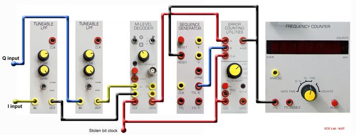
Figure 6: Decoder with error counting
Notice that, during setting up, the GATE of the FREQUENCY COUNTER is left permanently open by there being no connection to the TTL ENABLE socket.
T16 Repeat any or all of the above, as appropriate, with a longer sequence and different constellations.
TUTORIAL QUESTIONS
Q1 Sketch a section of an input sequence, and the corresponding encoded Q output signal from the M-LEVEL ENCODER switched to 4-QAM. Show clearly the framing, and the delay you measured between each frame and the coded output.
Q2 Show, in tabular form, the relationships between each frame word, and the corresponding Q and I output levels from the M-LEVEL ENCODER, for 4-PSK.
Q3 How many levels are there from each of the outputs of the M-LEVEL ENCODER module for an 8-PSK signal? If these cover the range ±2.5 volts, specify the levels for each of the points in the constellation of Figure 3. Repeat for other constellations. Compare with measurements.
APPENDIX
The digital divider in the BIT CLOCK REGEN module may be set to divide by 1
(inversion) , 2, 4, or 8, according to the settings of the on-board switch SW2.
| SW2-A (Left) | SW2-B (Right) | Divide by |
| DOWN | DOWN | 8 |
| DOWN | UP | 4 |
| UP | DOWN | 2 |
| UP | UP | -1 |
| Table A1: Switch selectable division ratios | ||