ECE 392 - Electrical Engineering Laboratory II
Lab 3: Common Emitter Amplifier
OBJECTIVES
Experience in design of a single stage amplifier. Simulation of circuit performance with Multisim and comparison with measured values.
DESIGN PRINCIPLES
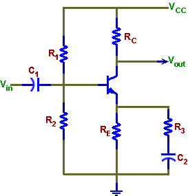
To work properly in an amplifier circuit a bipolar junction transistor (BJT) must be properly biased and operate in the active mode. This is achieved by a proper resistor network. The following conditions should be established:
- The collector should be biased half way between ground and VCC so
that the output can swing both way equally. This defines the value of RC
for a given collector quiescent current (with no input signal).
- The emitter should be biased at about 1 V to achieve temperature stability.
This defines the value of RE (assume that emitter and collector quiescent
currents are the same). Temperature stability comes from a negative feedback:
If the transistor heats up and the emitter current increases, the voltage
drop across RE increases, decreasing the voltage difference between the
base and the emitter, thus decreasing the current through the transistor
and lowering its temperature.
- Find the ratio of R1:R2 to put the base ~0.6V above the emitter (at
1.6 V).
- Chose R3 for the required gain G = RC/(RE ||
R3'),
where R3' =
R3+ re, with re ~ 50 Ω being the
"intrinsic emitter resistance".
- Select the values of C1 and C2 for the required f-3dB. Note that C1 is a component of an RC filter with Rin = Rb || β (R3+re). Rb is the equivalent resistance of the base biasing network (R1 || R2) and β ~ 100.

PRELAB
Design a common emitter amplifier following the schematic shown in the figure above (for more information see ref. 1)
Design requirements:
- Gain at quiescent point between 40 and 100, specified by the instructor
for each group;
- f-3dB must be not larger than 200 Hz;
- Vcc = 15 volts;
- Quiescent current Ic = 0.5 mA.
Specify component values to meet these requirements but check also the parts selection in your kit. Obtain components from other sources, if needed. You may deviate from the design specification by 10% if you do not find the required components.
Check your design by simulating circuit performance with Multisim using the same signals as you will use in the laboratory.
LABORATORY
1. ASSEMBLY AND TESTING
Wire the amplifier circuit following your design. Measure VE, VB, and VC in quiescent conditions. Drive the input with small sinusoidal signal (output should not exceed 1 V) and measure the values of the design parameters: small signal voltage gain, quiescent current, and the frequency f-3dB. Use DVM for accuracy but note the phase relation between input and output waveforms on the oscilloscope.
Measure also input and output impedances (Rin and Rout). To find input impedance, connect a series resistor to the input and measure voltage across it. The resistor should be large enough to measure the ac voltage across it. You may use the scope probes on the two ends of the resistor and measure the voltage displaying the difference between the two channels. To find output impedance, load the output with a resistor RL (through a capacitor – you need ac only!) and measure the output voltage drop due to the load. The voltage divider formula (with unknown Rout and known RL) will give you Rout.
NOTE: Circuits with high gain may oscillate. To prevent this, make neat and short connections between components and pay attention to grounding. Fixed resistors and capacitors are preferred to resistance and capacitance boxes.
2. FINE TUNING
If the measurements do not agree with the design parameters, fine tune your circuit by replacing or adding resistors. You may also introduce a trimming (adjustable) resistor for convenient tuning. Do not be concerned with obtaining an exact value of f-3dB as long as it is not larger than specified.
REPORT
In the report compare the design parameters with their measured values. Describe any fine tuning which had to be done on the circuit. Compare measurements with simulation results from Multisim, including the measured f-3dB vs. the value from simulated frequency distribution of the circuit. Compare measured and calculated values of input and output impedances.
To improve this amplifier you could expand this circuit by adding more stages (transistors).
What would you do to: (a) Increase the input impedance (b) Decrease the output impedance? Hint: recall previous experiments.
NOTE: You could use this amplifier in your project at the end of this laboratory course (audio, RF?)