ECE Undergraduate Laboratories
ECE 392 - Electrical Engineering Laboratory II
Lab 1: Field Effect Transistor; The J-FET
OBJECTIVES
Familiarity with basic characteristics and parameters of the J-FET.
Applications of J-FET as a current source and a variable resistor.
PRELAB
Draw a circuit for measurements of characteristics of a depletion mode, n-channel
JFET, described in part 1 of the Laboratory (below). Sketch basic characteristics
of a n-channel J-FET
(ID vs. VDS and ID vs. VGS) and
explain why it may be used as a constant current source and a voltage controlled
resistor. Indicate the parts of the characteristics where these functions can
be realized.
LABORATORY
Equipment needed from the stockroom: ECE 392 parts kit, analog universal meter,
resistance substitution box, leads.
1. JFET CHARACTERISTICS;
VP AND IDSS.
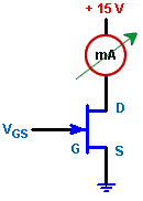
1. 1. Insert a JFET into the protoboard, connect the source
to ground and the drain to a 15 V power supply through an ammeter, which
will measure the drain current (ID). Measure this current for
different voltage values between the gate and the source (VGS). Use only negative voltage on the gate. Determine the pinch-off voltage
(VP), i.e. the gate voltage
at which the drain current is (practically) zero. Get a few measurements
at low current, with VGS close to VP so that you have
enough points on the logID vs. VGS graph to
determine VP. (see description of the report, below). Measure also IDSS, the drain current with VGS = 0. This current flows through the transistor when the gate connected to the source. Repeat measurements of VP and IDSS values for
another transistor of the same type in your kit and see if there is
significant difference between the two transistors. If so, make sure that
you can identify these transistors when you use them in other measurements.
1. 2. Next, measure ID(VDS)
characteristics of one of the transistors for VGS = 0 and two different
negative values. Note the linear part of the characteristics, where ID is
proportional to VDS (behaves like a resistor)
and the saturation part, where current is
(almost) independent of the voltage.
You will explore saturation range of the JFET transistor characteristic
in part 2 and the linear range in part 3, below.
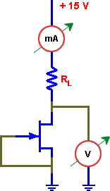
2. FET AS A CURRENT SOURCE.
The flat parts of the ID vs. VDS characteristics of
the FET allow to use this device as a simple constant current sources because
the current is (almost) independent of the voltage across it. Test this
idea with two transistors. Measure the current with different values of
the load resistor RL (100 Ω - 100 kΩ)chosen from
the resistance substitution box.
How good is this
current source? Determine the range of the load resistor values which
allows the current to stay constant within a given interval (say 2 % or
5%). What is the range of voltage across the transistor operating as a
current source.
You can buy JFETs with the gate connected to the source, so called
current regulator diodes. These two terminal devices, calibrated for
different current values, are current equivalents of Zener diodes which
provide a constant voltage.
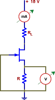
A variation of JFET current source, with self-biasing,
is shown on the next schematic. One of its advantages is that you
can obtain different current values by adjusting the resistor R (a
few k). Try this simple circuit and again determine the range of load
resistor RL which
allows you to keep the current constant.
Is this a better current source than the one without
a resistor? How does it work? Do you see feedback in this circuit?
What does the voltmeter here show?
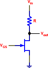
3. JFET AS A VARIABLE RESISTOR.
In the linear part of the JFET ID vs. VDS characteristics, the current through
the transistor is (roughly) proportional to the voltage across it, like in
a resistor. Moreover, the slope of these characteristics depends on VGS so
that changing the latter changes the value of the "resistance".
This effect can be used in many "voltage controlled circuits".
Experiment with the JFET as a variable resistor by using
it instead of a regular resistor in a two resistor voltage divider.
Chose
R = 10 k.
Apply a small sinewave signal (about 0.2 V) to
the input and observe variation of the output amplitude while changing
VGS (negative voltage must be used!). To see if the transistor
really behaves as a resistor, switch the waveform generator to a
triangular wave. Nonlinear dependence of voltage on current will
show as a distortion of the straight lines of the waveform. A resistor
has a linear I-V characteristic and will not distort a triangular wave.
From observation of the output waveform with a triangular
wave at the input
estimate in what range of input voltage the transistor behaves approximately
as a resistor? Explain your observation.
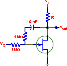
The circuit shown below is an improved version of a two resistor voltage
divider, with R a regular resistor and the transistor being an adjustable
resistor. The divider ratio can be adjusted by the control voltage VC.
A compensation circuit (between the output and the transistor gate) greatly
improves the circuit linearity as a part of output voltage (what fraction?)
is added to VGS. Check that this circuit behaves much better
as a voltage controlled resistive divider.
Compare the range of Vin with undistorted triangular
waveform with the previous case of the uncompensated circuit. Explain.
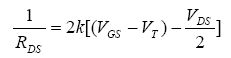
Hint:
The source drain resistance is:
where k is a constant. For linear behavior RDS must depend only on VGS.
REPORT
Describe briefly the measurements. Include all schematics. Show all results
with proper units. Do not forget to include the frequency used in ac measurements.
For part 1, make a graph of ID vs. VGS characteristic
and indicate the values of IDSS and VP on the graph.
VP is best determined from a plot of logID vs.
VGS. If you have data for two transistors, plot them on the same
graph. For part 2, you may plot ID vs. log RL to
cover a wide range of resistance. In the discussion, comment whether the parameters
IDSS and VP are the same for a given transistor type.. Address
the topics and answer the questions printed in bold letters in the manual. Add
any observations or conclusions you wish to make.
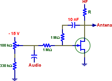
A PROJECT IDEA (OPTIONAL): ONE TRANSISTOR AM TRANSMITTER.
You could use the last circuit for amplitude modulation of a high frequency
carrier signal, just as it is done in AM radio transmission. Supply the input
with a high frequency sinewave (about 1 MHz) and modulate its amplitude by
feeding a low frequency signal (in the kilohertz range) through a capacitor
(~ 1 µF) to the slider of the potentiometer. The low frequency signal
may be picked up by an AM radio tuned to the appropriate frequency (in this
case about 1 MHz). If you supply an amplified signal from a microphone you
may hear your voice "on the air". A piece of wire attached to the
drain may serve as a transmitter antenna, extending the reception distance.