LAB 10: THE TRANSISTOR
COMPARISON OF TWO BASIC TYPES: MOS AND BIPOLAR
OBJECTIVES
Familiarity with MOSFET, the most used type of transistor today and its comparison with BJT. Demonstrating extremely high dc impedance of the MOSFET gate. Exploring linear characteristics and switching behavior of the transistors. MOSFET as voltage controlled device and BJT as current controlled device. MOS analog switch.
INTRODUCTION
There are two most common transistor types today: the Metal -Oxide - Semiconductor or MOS and the Bipolar Junction Transistor or BJT. The MOS is also designated as MOSFET because it is a field effect transistor (FET). A great majority of both types are made from silicon (Si) and a small fraction (about 2%) from gallium arsenide (GaAs). The BJT dominated the market initially but now most of the transistors, particularly in integrated circuits, are of the MOS type. The BJT, still holds its own, particularly in some analog and high power circuits. While most transistors of any type are made today as elements of integrated circuits (ICs), which can contain millions of circuit elements, single or discrete transistors are still useful in many applications like high frequency or power units.
In this laboratory we concentrate on the MOS transistor and compare it with the BJT. The important difference between the gate impedance of MOS and the base impedance of BJT is emphasized.. You will experiment with an N-channel enhancement mode power MOSFET and an npn type BJT.
PRELAB
A MOSFET is characterized by a very high input (gate) resistance. Does it mean that no appreciable current ever flows to the gate? Explain.
Draw schematics of circuits for experiments with a MOSFET described in sections 1, 2, and 3, below.
LABORATORY
Equipment needed from the stockroom: Proto-board, analog universal
meter, resistance substitution box, leads, scope probe.
1. POLARITY OF THE BIPOLAR TRANSISTOR
Check the base-collector and the base-emitter junctions with an ohmmeter
(use kΩ scale). You do not really measure a resistance but can identify the polarity of the transistor junctions. Verify that the npn transistor has the corresponding junctions between the emitter (n-type) and the base (p-type), and between the base and the collector (n-type).
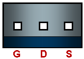
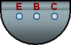
Fig 9.1: Terminal connections to MOS (left) and BJT (right) transistors.
2. TRANSISTOR AS A SWITCH
2.1 BJT
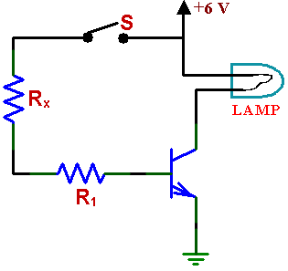
Assemble a circuit (shown below) in which an npn BJT is used to switch
on and off a small incandescent lamp. Resistor R1 should be 220 to 390 ohms to protect the transistor base from excessive current. Rx may be a resistance substitution box.
Fig. 9.2 Transistor switch circuit.
In this application a small current in the base circuit controls a larger
current in the collector circuit (the lamp). In this way high power transistors
can be used to control large current loads.
Find the value of the base resistor Rx which allows turning on the lamp to its full brightness. Measure the base voltage Vb when the lamp is “on” and calculate the base current that was used to turn on fully the BJT. What is the equivalent resistance between the base and the emitter of the transistor in this configuration? Measure also the lamp current and the collector voltage. Calculate also the equivalent resistance between the emitter and the collector when the transistor is “on”.
2.2 MOSFET
WARNING: You are about to work with a MOSFET, a device that is very sensitive to static electricity. Do not touch the gate lead with your hand before touching first one of the other two transistor leads with the same hand. When the transistor is inserted in a proto-board, “ground” your body first by touching the circuit board before touching the gate electrode. Keep the transistor inserted in the black conducting foam pad when not in use.
Replace the BJT with an n-channel enhancement mode MOSFET: the gate terminal replaces the base, the source replaces the emitter and the drain the collector (see Fig. 9.1) Turn the lamp “on” and “off” by connecting resistor Rx either to the positive power supply terminal or to the ground.
Now a surprise: disconnect the gate resistor from either ground or power supply. Touch the free end of the resistor (or the transistor gate terminal) with one hand and touch your other hand to either ground or the positive terminal. When the lamp turns “on” remove your hands and wait. After a while “ground” the gate with your fingers. From now on you should remember never leave the MOSFET gate unconnected. What can you say about the input resistance of this circuit? Do you need much current to turn the transistor “on”? Compare with BJT!
Measure also the lamp current and the drain voltage. What is the output resistance (resistance between source and drain) of this circuit?
NOTE: The transistor used in these experiments is a power MOSFET capable of carrying a large current and having relatively low channel resistance. A MOSFET used typically in digital circuits would not turn on the bulb; its channel resistance is too high. It could however control an LED (Light Emitting Diode) which requires much less current than a light bulb.
2.3. SWITCHING OPERATION OF A MOSFET.
Replace the light bulb in the MOSFET circuit by two parallel 100 ohms resistors. Apply a square wave from a waveform generator at your bench to the gate through a 10 k resistor. The amplitude should be large enough to switch the transistor on and off but use also the generator dc bias adjustment to obtain one polarity output (check on the scope). Increase the frequency from about 1 kHz and observe the input signal at the gate and the output signal on the drain. Why do you really need a scope probe here? Part of the input signal should look like an RC curve. Try to estimate the gate capacitance.
NOTE: The input circuit consisting of the resistor and the gate is more complicated than a simple RC circuit because it is affected by the voltage on the drain. As the drain voltage swings it influences the gate voltage (feedback) and the effect looks like changing capacitance of the gate. This explains the somewhat strange shape of the observed waveforms.
To find how fast the transistor can switch, eliminate the gate resistance and connect the gate directly to the waveform generator. Beware of static electricity!
Increase the frequency and observe the waveforms. Measure the “turn on” and “turn off” times at both the input and the output. What limits the switching speed? Is there any resistance in the input circuit?
3. TRANSISTOR AS AN AMPLIFIER
3.1 MOSFET
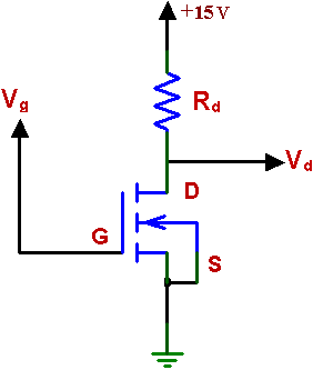
Since a MOSFET gate practically does not draw any current, the output current of this device is controlled by the gate voltage. To examine this effect measure the drain current as a function of gate voltage, with a grounded source. Use the circuit in Fig. 9.3 where the drain resistor Rd could be 1k. Increase the gate voltage Vg from zero while monitoring drain voltage. Vd. Calculate drain current and plot its dependence on Vg. Determine the threshold voltage of the transistor.
Fig. 9.3: Common source MOSFET circuit.
3.2 BJT
A BJT can controlled by base current and the purpose of this measurement is to demonstrate the so called transistor’s “current gain”, or the ratio of collector current to base current. The current gain (β or hFE) is not a good transistor parameter because it depends on operating conditions and varies widely for different specimens of the same type but it demonstrates an important function of a transistor: amplification.
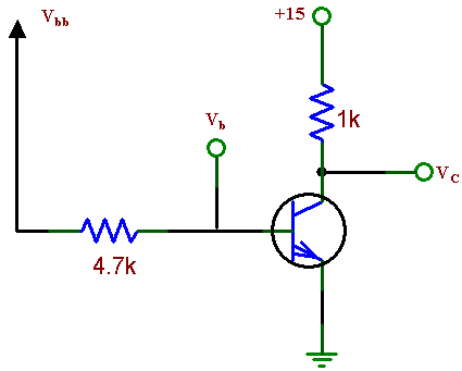
Measure the transistor current gain for a few values of IB, using the circuit shown in Fig.9.4, below.
Fig. 9.4 Circuit for measurement of current gain.
You have several options in making these measurements. Measuring Vb and Vbb with a digital voltmeter, you can determine base current if the value of the base resistor is known (4.7k in Fig. 9.4). Alternatively, you can measure base current directly with a digital ammeter. The collector current can be determined by measuring collector voltage Vc or it may be measured directly by inserting an analog ammeter in series with the 1k resistor. The digital meter will be needed for measuring Vb or the current in the base.
Make measurements for several values of base current IB by changing Vbb. Tabulate results including base-emitter voltageVBE and collector emitter voltage VCE as well as calculated values of current gain (hFE or beta).
4. TRANSISTOR CHARACTERISTICS
Using a curve tracer test both MOS and BJT transistors in common source or emitter mode, respectively. The characteristic curves include drain (collector) current as a function of drain (collector) voltage for different gate voltage (base current) values. Choose voltage and current ranges which include the values you measured in part 3. Sketch the observed curves labeling the axes and indicate approximate scales of the axes. Relate the curves to the values measured in part 3.
5. MOSFET AS AN ANALOG SWITCH
A very useful circuit, impossible with BJTs, can be built with MOSFETs used as switches of analog signals. They act as solid state relays controlled by the gate voltage, while standard relays are controlled by current in their coils. Such circuits, used in data acquisition systems, serve as analog multiplexers which allow selection of one of the several data inputs. In other applications they may change gain of an operational amplifier or an attenuation ratio by switching different resistors, using the control voltage levels set usually by digital circuits. There are special CMOS analog switches, made as integrated circuits in multiple units, called also transmission gates. Here we start experiment with analog switches using our power MOSFET.
Build an analog switch using a MOSFET. Supply the signal to the source and take output from a resistor (between 10k and 100k) connected between the drain and ground. Control voltage should be supplied to the gate through an ordinary SPDT switch. Supply a waveform, riding on some dc bias from a generator to the input and observe the output on a scope while changing the switch position. Adjust the dc bias control on the generator and observe its effect. What should be the relation between the control voltage level supplied to the gate and the input voltage level for this device to work?
REPORT
Include all schematics with the values of the components.
Present clearly all graphs.
Address all issues and questions printed in bold letters in the text.
What major differences you observed in operation of MOSFET and BJT?