ECE Undergraduate Laboratories
ECE 394 - Digital Systems Laboratory
Lab 7: Memory and ALU
PART A: Memory
1. Introduction
Generally speaking, memory elements can be divided into two categories.
One is called Random Access Memory (RAM), and the other is called Read Only
Memory (ROM).
RAM circuits on the market have different configurations depending upon how the memory cell array is organized. A memory cell array organized with N by M cells can store N words with each word being M bits long. For example, the IC type 7489 is a 16 by 4 RAM chip. It can store up to 16 different words, and each word is 4 bits long. Apart from memory cell array, RAM circuits also need address decoding logic and read/write control logic. The address decoding logic translates the data address (usually in binary format) into the physical location of a particular word in the memory cell array. Therefore, the memory cells in the specified memory word are activated and ready to either put the data on to the data output pins (read process), or to receive data from the data input pins (write process). Whether the process is read or write depends upon the read/write control logic. Read and write processes are also referred to as data fetch and data load respectively.
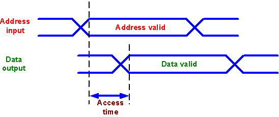
ROM circuits are similar to RAM circuits except that data are already stored permanently in the memory cell array. Only the read process is allowed. Therefore ROMs do not have the read/write control logic. The PROM, programmable ROM, holds semi-permanent data; data can be modified, but slowly. One important measure for a memory element is its access time. In order to read data, an appropriate address must be applied to the address inputs, and perhaps an enable signal asserted. After a short period of time, the data are valid on the output pins. The short time period is called the access time of the memory. Access time of a memory reflects how fast the memory can respond to the request for data. Fig. 1 illustrates how access time is measured assuming all enable signals are asserted true.
Fig.1: Access time of memory chip.
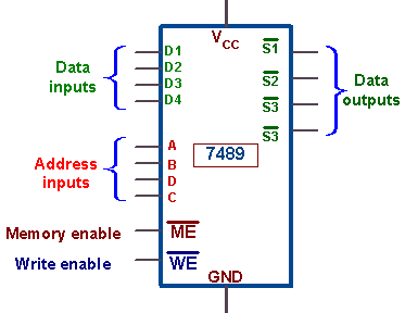
The IC chip you are going to use in this experiment is 7489. 7489 is a 16 by 4 random access memory. Its pin assignment to the inputs and outputs is shown in Fig. 2. The four address inputs select one of the 16 words in the memory. The least significant bit of the address is A, and the most significant bit is D. The read/write control logic has two control inputs. The memory enable ( ME )
input must be equal to low to enable the memory. If ME is
high, the memory is disabled and all four outputs are at high impedance
level. The write enable ( WE ) input
determines the type of operation as indicated in the function table. The
write operation is performed when WE is
low. This is a transfer of the
binary data from the data inputs lines into the selected word in memory. The
read operation is performed when WE is
high. This transfers the value stored in the selected word into the output
data lines (complemented). The inverted outputs are open-collector to allow
external wired logic for memory expansion.
ME
WE
Operation
Data Outputs
L
L
Write
Complement of data inputs
L
H
Read
Complement of selected word
H
X
Disable
High impedance
Fig. 2. 7489 16x4 RAM
2. Objectives
Through the lab experiments students are expected to become familiar with the structure and the working mechanisms of memory elements. Students will learn the concept of data load and data fetch, and how to measure memory access time.
3. Experiments
3.1. Testing the RAM
An open-collector gate requires an external resistor for proper operation. However, an open-collector gate can be operated without an external resistor if its output is connected to the input of another gate. Since the outputs of the 7489 produce complemented values, we might as well insert four inverters to change the outputs to their normal values and, at the same time, avoid the need for external resistors.
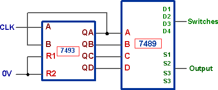
Now connect the address inputs to a binary counter using IC type 7493
as shown in Fig. 3. Connect the four data inputs to toggle switches
and the data outputs to four 7404 inverters. Provide four LEDs for
the address and four more for the outputs of the inverters. Connect ME to
ground and WE to a pulser that provides
a negative pulse. Store
a few words into the memory and then read them to verify that the write
and read operations function properly. Leave the WE in
the read mode (high), unless you want to write into memory. The proper
way to write is first set the address using the counter and the inputs
with the four toggle switches. To store the word in memory, pulse
the WE switch to the write position. Be
careful not to change the address or the inputs when WE is
asserted.
Fig. 3. Setup for testing the 7489
3.2. Measuring the Access Time
First store the value 0000 and 0001 at address 0000 and 0001 respectively. Disconnect the counter from the memory. Now connect the address bits B, C, and D to ground. Connect the address bit A (the least significant bit) to a square wave of 1 MHz. Make sure the square wave oscillates between 0V and 5V. Connect both the square wave and the least significant bit of the data outputs (S1) to the scope to compare their rising and falling edges. What is the access time for your chip?
3.3. Memory Expansion
Expand the memory unit to a 32 by 4 RAM using two 7489 ICs. Use
the ME inputs to select between the two ICs. Note that
since the data outputs are open-collector, you can tie pairs of terminals
together to obtain a logic wired-OR operation in conjunction with the output
inverter.
4. Equipment and parts required
Protoboard
Oscilloscope
Signal generator
Two TTL 16x4 RAM (7489)
One TTL binary counter (7493)
One TTL inverter (7404)
Four LEDs and limiting resistors
One TTL ALU (74181) (for part B)
PART B: Arithmetic Logic Unit
1. Introduction
The Arithmetic Logic Unit (ALU) is the kernel block of a central processing unit (CPU). The ALU can perform various arithmetic operations such as parallel addition and subtraction. You have already learned the adder structure in Experiment 4. The adder introduced in Experiment 4 is a one-bit adder. However, data to be handled and processed in the ALU are often represented by several bits (usually the width of a CPU word). Using the adder in Experiment 4 to process one bit at a time would be too slow. Therefore the ALU is normally required to have the ability to perform parallel addition and subtraction, so that addition and subtraction of several bits can be performed simultaneously. Apart from speed, the ALU is also required to have flexibility. The function of the ALU can be controlled or programmed to carry out different arithmetic functions.
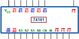
The ALU device used in this experiment is 74181 and its pin assignment
is shown in Fig. 4. 74181 consists of four parallel full adder/subtractor
circuits. Data applied on the inputs Ai’s and Bi’s are
processed and the sum or difference is available at the output in a parallel
format. Selection of the desired ALU function is controlled by five
control lines, S0–S3, and mode, M
Fig. 4. 74181 4-bit ALU
2. Objectives
Students are expected to become familiar with the basic functions of the ALU. This experiment will also help students understand parallel data handling.
3. Experiments
3.1. Parallel Adder
Connect A0-A2, and B0-B2 to six switches. Connect A3 and B3 to the ground and F0-F3 to four LEDs. The select lines S0-S3, mode M, and carry-in signal CN, are set to the addition function. Note that A0 and B0 are the LSBs of the input data, and A3 and B3 are the MSBs of the input data. F0 and F3 are respectively the LSB and MSB of the output data. Now perform the addition function of 74181 by setting the input switches to the appropriate values as shown in Table 1. Record the output data from the LEDs (when an LED lights up, it indicates the output is logic high) and verify the outcomes.
Table 1. Inputs for addition, F = A + B
A2
A1
A0
A
B2
B1
B0
B
F3
F2
F1
F0
F
0
0
0
0
0
0
0
0
0
0
1
1
0
0
0
0
0
1
0
2
0
0
0
0
0
1
1
3
0
0
0
0
1
0
0
4
0
0
0
0
1
0
1
5
0
0
0
0
1
1
0
6
0
0
0
0
1
1
1
7
0
0
0
0
1
1
1
7
0
0
1
1
1
1
1
7
0
1
0
2
1
1
1
7
0
1
1
3
1
1
1
7
1
0
0
4
1
1
1
7
1
0
1
5
1
1
1
7
1
1
0
6
1
1
1
7
1
1
1
7
Change the connection for select lines to the subtraction function and perform the subtraction function by setting the input switches to the appropriate values as shown in Table 2. Record the output data from the LEDs and verify the outcomes.