ECE Undergraduate Laboratories
ECE 394 - Digital Systems Laboratory
Lab 4: Shift Registers
1. Introduction
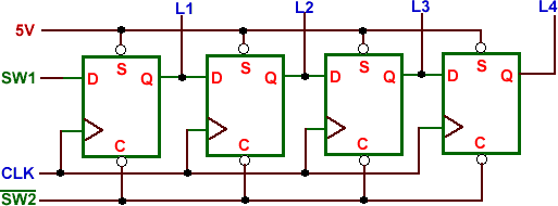
A shift register is an n-bit register with provision for shifting its stored data by one position at each clock pulse. The logical configuration of a shift register consists of a chain of flip-flops connected in cascade, with the output of one flip-flop connected to the input of the next flip-flop. All flip-flops receive a common clock pulse which causes the shift from one stage to the next. Fig. 1 shows a simple shift register configuration. The new bit to be shifted into one end must be specified, and the bit shifted off the other end is lost unless it is saved externally. Although Fig. 1 shows a right-shift register, the same register can obviously be used for left shifts simply by reversing the sense of the bits. Most shift registers have provision for shifting only in one direction, but some have a control input that allows either left or right shifting to be specified at each clock.
Fig. 1. 4-bit shift register.
One way to load n bits of data into the flip-flop chain is to load the data one bit each clock cycle using the serial input. Some shift registers also have parallel inputs that can be used to load all n bits in one clock cycle. The output of a shift register can be observed one bit at a time at the serial output, but some shift registers also have parallel outputs for observing all n bits at once.
Shift registers are classified according to three basic considerations: their method of data handling (serial-in serial-out, serial-in parallel-out, and parallel-in serial-out), their direction of data movement (shift right, shift left, and bidirectional), and their bit length. One of the important applications of shift register circuits is in serial computation. Compared to parallel computation, where all bits in a word are processed at the same cycle, serial computation process words in one bit per cycle. Therefore, serial computation is slower, but it has the advantage of requiring less hardware and wiring. A serial adder will be built in this experiment as an example.
2. Objectives
Students are expected to understand various data handling methods in shift
registers and their usage.
3. Experiment
3.1. 4-bit Shift Register
Use two 7474 dual flip-flops to connect a serial-in, parallel-out shift
register as shown in Fig. 1. Connect L1–L4 to four LEDs (with current-limiting resistors), SW1
and
SW2 to switches, and CLK to a
pulser. Initially, set
SW2 to logic 1. Switch
SW2 being at logic 1 clears all flip-flops. Now set SW1 to logic
1 and
SW2 to logic 0. Push the pulser button several times to allow
more logic 1 to be shifted into the shift register. Change SW1 to
logic 0 and repeat the experiment again.
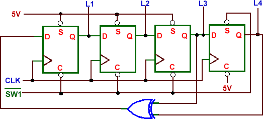
3.2. Pseudo-random Sequence Generator
Now use the above circuit to build a pseudo-random binary sequence generator
as shown in Fig. 2. This binary sequence generator will display a
random output (repeats every 2n–1 bits, where n is the number of
flip-flops used in the shift register). The IC 7486 provides the
exclusive-OR needed in the circuit. To start the sequence generator,
set the initial state of the shift register to 0001 by setting the switch
SW1 to logic 1. Then change
SW1 to logic 0 as this will release the control input. Now apply
the clock and record the output in a table. Does the output show
randomness? Does the output repeat after 15 pulses?
Fig. 2. Pseudo-random binary sequence generator.
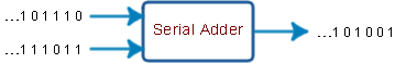
3.3. Serial Adder
A serial adder adds bits adds a pair of binary numbers serially with a simple full adder. The carry out of the full adder is transferred into a D flip-flop and the output of this carry flip-flop is then used as the input carry for the next pair of significant bits. Fig. 3 illustrates an example of serial addition.
Fig. 3 Serial addition.
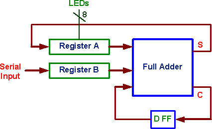
Fig. 4. shows the block diagram design of a serial adder. The two binary numbers to be added serially are stored in two shift registers (using two 74164, 8-bit serial-in, parallel-out shift registers). Bits are added one pair at a time through a single full adder (such as the one in Experiment 2) The carry out of the full adder is transferred into a D flip-flop. The output of this carry flip-flop is then used as the input carry for the next pair of significant bits. The sum output from the full adder is transferred into register A as the contents of the register are shifted out.
To perform the addition, the following steps are used.
1. Shift the first 8-bit augend into A (remember to shift in LSB first)
and addend into B. This is done by performing the following steps:
Clear registers A and B, and the D flip-flop. The registers and flip-flop have a clear input that can be used to accomplish this task.
Shift the augend through the serial input. For 8-bit registers, one bit will be shifted into register B for each of eight clock cycles, least significant bit first. (Since registers A and B initially contain all zeroes, the output of the full adder will be 0 for both the sum and carry outputs during these clock cycles. You can either load these zeroes into register A or just leave A unchanged. In either case, after eight clock cycles, Register B will contain one operand and register A will contain all zeroes.
Shift the addend through the serial input. This is actually two tasks performed at once. While the addend is being shifted into register B, the augend is being shifted out of B and into register A. To understand how this occurs, recall that register A contains all zeroes. Whatever bit is being shifted out of B is being added to the zero in the least significant bit of A. The sum will just be the least significant bit of B, which is shifted into the most significant position of register A. After eight clock cycles, register A contains the augend and register B contains the addend.
2. Clear the D flip-flop and run the adder for eight cycles to obtain
the sum.
Fig. 4. Block diagram of a serial adder.
Table 1 shows the values in registers A and B when the data values 01011101 and 10011110 are added together.
Table 1: Trace of the serial adder
Serial Input
Register A
Register B
D FF
Comments
X
00000000
00000000
0
Clear A, B, D
1
00000000
10000000
0
0
00000000
01000000
0
1
00000000
10100000
0
1
00000000
11010000
0
1
00000000
11101000
0
0
00000000
01110100
0
1
00000000
10111010
0
0
00000000
01011101
0
Augend in B; 0 in A
0
10000000
00101110
0
0+1=1
1
01000000
10010111
0
1
10100000
11001011
0
1
11010000
11100101
0
1
11101000
11110010
0
0
01110100
01111001
0
0
10111010
00111100
0
1
01011101
10011110
0
Augend in A; Addend in B
X
10101110
X1001111
0
C=0, S=1
X
11010111
XX100111
0
C=0, S=1
X
01101011
XXX10011
1
C=1, S=0
X
10110101
XXXX1001
1
C=1, S=1
X
11011010
XXXXX100
1
C=1, S=1
X
11101101
XXXXXX10
0
C=0, S=1
X
11110110
XXXXXXX1
0
C=0, S=1
X
11111011
XXXXXXXX
0
Sum in A
4. Prelab
Show the sequence generated by the pseudo-random sequence generator.
Study the operation of the 74164.
Draw a circuit diagram of the serial adder showing the connections
for all the components.
What is the maximum clock speed for the adder circuit of part 3.3? Assume worst case delays and 74LSXX type logic.