ECE Undergraduate Laboratories
ECE 394 - Digital Systems Laboratory
Lab 8: Design Project – 4-bit RPN Calculator
1. Objectives
This project is designed to allow students to apply digital design techniques discussed in the previous experiments. The objective is to design a simple 4-bit reverse polish notation (RPN) calculator. The components used consist of counters, multiplexers, 16x4 RAMs, 4-bit ALU and PLD.
2. Description
Reverse Polish Notation (RPN) is a notation for representing arithmetic formula. The common
notations that we are familiar with had the operator placed in between the two operands
(called the infix notation), for example, A + B, A * B, A + B + C. The RPN notation
(or postfix notation) places the operator at the end of the operands, for example,
A B +, A B *, A B + C +. The RPN notation has the advantage that it can express
operation precedence without using parentheses. For example,
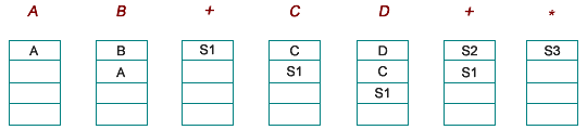
Expression in infix notation: (A + B) * (C + D)
Same expression in postfix notation: A B + C D + *
RPN has been popularized in calculators made by HP. A stack implementation is typically
used to evaluate an expression in RPN. For example, to calculate A B + C D + *
Scanning the RPN expression from left to right
If it is an operand, it is pushed onto the stack.
If it is an operator, the top two items on the stack are popped and evaluated with the
operator; the result is pushed back onto the stack.
S1 = A + B
S2 = C + D
S3 = S1 * S2
3. Requirement
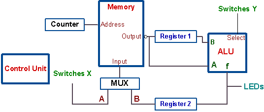
Fig. 1 shows the block diagram design of the calculator. The 16x4 RAM serves as the
stack of the RPN calculator and a 4-bit up/down counter is used as the stack pointer. Data can be entered into the stack through the switches X. To perform a calculation, the operands are first pushed into the stack and the desired function is selected with switches Y. The control unit of the calculator then goes through a sequence of steps to perform the operation. The final result is stored back into the RAM.
Fig. 1. Block diagram design of a 4-bit RPN calculator
The sequence of events that happens for each operation
is as follows:
PUSH – push an operand into the stack.
Data are selected with switches X.
1. Increment the counter.
2. Write data into the memory.
FUNCTION – perform a calculation.
The function to be performed is selected with switches Y.
1. Data from RAM output is latched into register 1
2. Decrement the counter.
3. Result is latched into register 2.
4. Write data into the memory.
The control signals which are generated by the control unit are listed in
Table 1.
Table 1. Control signals for RPN calculator.
Counter
Memory
Register1
Register2
ALU
MUX
Operation
Up
Down
ME
WE
Enable
Enable
Select
Select
1
0
0
1
0
0
*
*
PUSH
0
0
0
0
0
0
*
A
0
0
0
1
0
0
*
A
0
0
0
1
1
0
function
*
FUNCTION
0
1
0
1
0
1
function
*
0
0
0
0
0
0
function
B
0
0
0
1
0
0
function
B
Note. This table is just for reference, you should decide the exact signals
according to what kind of chips you use.
The control circuit can be implemented by a state machine, memory lookup
table, or can be generated using a PLD. Either design is acceptable.
4. Prelab Assignments
1. Design the control unit that would generate the control signals shown
in Table 1.
2. Draw a circuit diagram of the calculator showing the connections for
all the components.