Lab 7: Microcoded CPU Design
Objectives:
The objective of this experiment is to design and implement a microcoded CPU using the ALTERA DE2 board. A VHDL program with a structural description will be developed to model the CPU. This experiment will also familiarize the student with the lpm library components.
Preparation
Review Chapter 7 of Computer Systems Organization & Architecture by John Carpinelli.
References
- John D. Carpinelli, Computer Organization & architecture, Addison Wesley, 2001.
- Morris Mano, Computer Engineering, Hardware Design, Addison Wesley.
Equipment Needed
- ALTERA DE2 Board
- Signal generator for clock
Background
In this experiment, the student will design a microcoded CPU based on the ALTERA DE2 doard. A VHDL program based on a structural description will be develop to model CPU. You must use the lpm library components to design the CPU and the RAM. Two components, the ALU and a simple microsequencer based on Experiment 2 will be provided.
CPU Specifications
The CPU has the following specifications:
- The CPU can access 256 8-bit words of RAM. This implies that an 8-bit Memory Address Register (MAR) and an 8-bit Program Counter (PC) are needed
- The CPU accesses the 8-bit memory via an 8-bit Memory Data Register (MDR)
- The CPU has two internal 8-bit registers: the accumulator (A) and a general-purpose register (R)
- The CPU has a 1-bit condition flip-flop (Z), which derives its input as described below
- The CPU is capable of executing the instructions shown in Table 7.1 (The
instructions shown in
italics are for extra credit.) Note that V is defined as the logical OR of
the bits of A; this is
similar in function to a zero flag. Also note that LOAD, LOADSP, STORE, JUMPZ
and JUMP
use 8-bit address (Γ) as part of the instruction code. In addition
to the CPU design, your VHDL
code must include a 256 words 8-bit RAM for programs and data.
- Extra credit: Implement the LOADSP, PUSH and POP instructions, along with the 8-bit stack pointer (SP) used by these instructions.
| Table 7.1: CPU instruction set. | ||
|---|---|---|
| Instruction code | Instruction | Function |
| 00000000 | NOP | No operation |
| 00100000Γ | LOAD Γ | A ← M[ Γ ] |
| 00110000Γ | STORE Γ | M[ Γ ] ← A |
| 01000000 | MOVE | R ← A |
| 01010000 | ADD | A ← A + R |
| 01100000 | AND | A ← A and R |
| 01110000 | TESTNZ | Z ← not V |
| 01110001 | TESTZ | Z ← V |
| 10000000Γ | JUMP Γ | PC ← Γ |
| 10010000Γ | JUMPZ Γ | if (Z=1) then PC ← Γ |
| 11000000Γ | LOADSP Γ | SP ← Γ |
| 11010000 | PUSH | M[--SP] ← A |
| 11100000 | POP | A ← M[SP++] |
| 11110000 | HALT | PC ← 0, stop microsequencer |
ALU and microsequencer
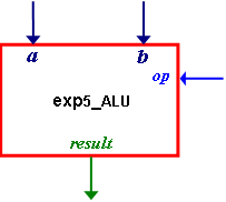
Two components are provided to reduce the complexity of this experiment. A 2-function (add and logical-and) 8-bit ALU is provided and is shown in Figure 7.1. The component declaration for the ALU is as follows:
component exp7_alu is
port (a, b: in std_logic_vector(7 downto 0);
op: in std_logic_vector(0 downto 0);
result: out std_logic_vector(7 downto 0));
end component;
where a and b are the 8-bit inputs, result is the 8-bit output and op is a 1-bit function selection:

The VHDL code for the ALU is included in Appendix 7.1. A simple microsequencer is also provided (Figure 7.2). The component declaration for the microsequencer is as follows:
component exp7_useq is
generic (uROM_width: integer;
uROM_file: string);
port (opcode: in std_logic_vector(3 downto 0);
uop: out std_logic_vector(1 to (uROM_width-9));
enable, clear: in std_logic;
clock: in std_logic);
end component;
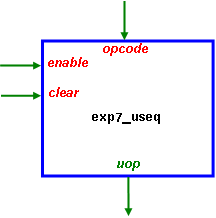
The microsequencer contains a 256-word micro-ROM. The width of each micro-ROM word is declared through the parameter uROM_width. The parameter uROM_file is the name of the mif (memory initialization file) for the contents of the micro-ROM. The organization of the content of the micro-ROM is shown in Figure 7.3.
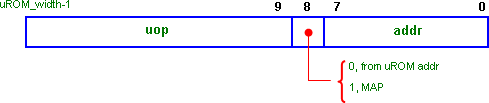
The lower order 8-bit (bits 7 through 0) is the address of next microinstruction when bit 8 is 0. If bit 8 is 1, then the next microinstruction address is obtained through a mapping function. The mapping function generates an 8-bit value by concatenating the 4-bit opcode input with “0000”. The length of the micro-operation field equals to (uROM_width – 9). For example, if uROM_width is 20, then uop goes from 1 to 11 that corresponds to bits 19 through 9 of the micro-ROM content. The other 3 inputs to the microsequencer are:
- clock – the system clock.
- enable – enables the microsequencer so that transitions can occur.
- clear – resets the address register in the microsequencer to 0.
The VHDL code for the microsequencer is included in Appendix 7.2. The 256x8 RAM should be implemented with the lpm library component, lpm_ram_dq.
Prelab Assignment
- Prepare a preliminary hardware block diagram design for your CPU. Explain the purpose of the blocks and components.
- Prepare a preliminarily commented version of the microcode for your system.
Lab Assignment
Develop VHDL code using a structural approach for the CPU described above. Program, debug and test your design. For final demonstration, your CPU should be able to run all the test cases and display the result of A using the two 7-segment displays on the DE2 board.
See Appendix 7.1 and Appendix 7.2 in the appendixes section