Lab 2: Introduction to Altera DE2 Board
Objectives:
The objective of this experiment is to gain an understanding of the Altera DE2 Board and create a simple project using input switches and the output LEDs.
Preparation
- Review the provided user manual and tutorials for the Altera DE2 Board
Equipment Needed
- ALTERA DE2 Board
References
Background
A field programmable gate array (FPGA) is a semiconductor device containing programmable logic components and programmable interconnects. The programmable logic components can be programmed to duplicate the functionality of basic logic gates such as AND, OR, XOR, NOT or more complex combinational functions such as decoders or simple math functions. In most FPGAs, these programmable logic components also include memory elements, which may be simple flip flops or more complete blocks of memories
For this course we will be using a programming language called VHDL to program the FPGA found on the Cyclone 2 chip on your Altera DE2 Board. VHDL is a very robust language that can be implemented in a very high level format, using programming concepts such as for loops, if-then statements, and case assignments. VHDL also includes libraries that define adders, subtracters, counters, flip-flops, and more that can be instantiated to create a structural approach to your code.
The purpose of this exercise is to learn how to connect simple input and output devices to an FPGA chip and implement a circuit that uses these devices. We will use the switches SW17−0 on the DE2 board as inputs to the circuit. We will use light emitting diodes (LEDs) as outputs to your device.
The DE2 board provides 18 toggle switches, called SW17−0, which can be used as inputs to a circuit. There are also 18 red LEDs, called LEDR17−0, which can be used to display output values. The DE2 board has hardwired connections between its FPGA chip and the switches and lights. To use SW17−0 and LEDR17−0 it is necessary to include in your Quartus II project the correct pin assignments, which are given in the DE2 User Manual.
Part 1
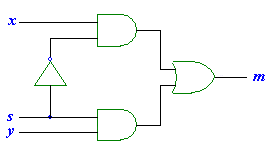
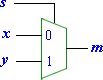
Figure 2.1 shows a sum-of-products circuit that implements a 2-to-1 multiplexer with a select input s. If s = 0 the multiplexer’s output m is equal to the input x, and if s = 1 the output is equal to y. Part (b) of the figure gives a truth table for this multiplexer, and part (c) shows its circuit symbol.
 |
|
 |
||||||
| a) Circuit | b) Truth Table | c) Symbol | ||||||
|---|---|---|---|---|---|---|---|---|
Figure 2.1: A 2-to-1 multiplexer |
||||||||
The multiplexer can be described by the following VHDL statement:
m <= (NOT (s) AND x) OR (s AND y);
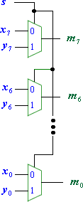
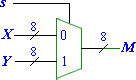
You are to use the provided VHDL entity in appendix 2.1 that describes the circuit given in Figure 3a. This circuit has two eight-bit inputs, X and Y, and produces the eight-bit output M. If s = 0 then M = X, while if s = 1 then M = Y. We refer to this circuit as an eight-bit wide 2-to-1 multiplexer. It has the circuit symbol shown in Figure 3b, in which X, Y, and M are depicted as eight-bit wires.
 |
 |
| a) Circuit | c) Symbol |
|---|---|
| Figure 2.2: An eight-bit wide 2-to-1 multiplexer | |
Part 2
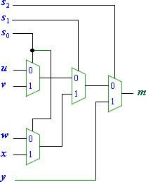
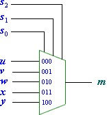
In Figure 2.1 we showed a 2-to-1 multiplexer that selects between the two inputs x and y. For this part consider a circuit in which the output m has to be selected from five inputs u, v, w, x, and y. Part (a) of Figure 2.3 shows how we can build the required 5-to-1 multiplexer by using four 2-to-1 multiplexers. The circuit uses a 3-bit select input s2s1s0 and implements the truth table shown in Figure 4b. A circuit symbol for this multiplexer is given in part (c) of the figure.
 |
|
 |
||||||||||||||||||||||||||||||||||||
| a) Circuit | b) Truth Table | c) Symbol | ||||||||||||||||||||||||||||||||||||
|---|---|---|---|---|---|---|---|---|---|---|---|---|---|---|---|---|---|---|---|---|---|---|---|---|---|---|---|---|---|---|---|---|---|---|---|---|---|---|
| Figure 2.3: A 5-to-1 multiplexer | ||||||||||||||||||||||||||||||||||||||
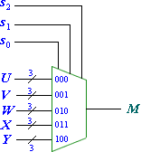
Recall from Figure 2.2 that an eight-bit wide 2-to-1 multiplexer can be built by using eight instances of a 2-to-1 multiplexer. Figure 2.4 applies this concept to define a three-bit wide 5-to-1 multiplexer. It contains three instances of the circuit in Figure 4a. The VHDL code for this circuit is given in appendix 2.1
 |
|
Prelab Assignments
- Review the manual and tutorials for the Altera DE2 Board.
- Understand how to create and compile projects.
- Review how pin assignments are done.
- Review how to program the Altera DE2 Board.
Lab Assignments
Part 1
- Create a new Quartus II project for your circuit.
- Include the given VHDL code for the eight-bit wide 2-to-1 multiplexer
in your project.
Use switch SW17 on the DE2 board as the s input, switches SW7−0 as the X input and SW15−8 as the Y input. Connect the SW switches to the red lights LEDR and connect the output M to the green lights LEDG7−0. - Include in your project the required pin assignments for the DE2 board.
- Compile the project.
- Download the compiled circuit into the FPGA chip. Test the functionality of the eight-bit wide 2-to-1 multiplexer by toggling the switches and observing the LEDs.
Part 2
- Create a new Quartus II project for your circuit.
- Include the given VHDL code for the three-bit wide 5-to-1 multiplexer. Connect its select inputs to switches SW17−15, and use the remaining 15 switches SW14−0 to provide the five 3-bit inputs U to Y. Connect the SW switches to the red lights LEDR and connect the output M to the green lights LEDG2−0.
- Include in your project the required pin assignments for the DE2 board. Compile the project.
- Download the compiled circuit into the FPGA chip. Test the functionality of the three-bit wide 5-to-1 multiplexer by toggling the switches and observing the LEDs. Ensure that each of the inputs U to Y can be properly selected as the output M.