Lab 1: Event Driven Circuit
Objectives:
The objective of this laboratory is to familiarize the student with the design techniques for event driven sequential circuits, and to introduce the student to applications involving EEPROMs.
Preparation:
Review Chapter 2 of Computer Systems Organization & Architecture by John Carpinelli.
Equipment Needed
- One switch block
- Red, amber, and green LEDs
- One protoboard
- One 2816 EEPROM
- One 74374 octal D-type latch (or CMOS equivalent)
- Signal generator for clock
References
John D. Carpinelli, Computer Systems Organization & Architecture, Addison Wesley, 2001.
Morris Mano, Computer Engineering Hardware Design, Addison Wesley.
Background
Event driven sequential circuits differ from combinatorial circuits in that the outputs of the circuit depend not only on the present state of the inputs but also on the past history of the inputs. Thus a sequential circuit has memory. Memory is provided for each bit needed to define a state by using a bit storage device such as a flip-flop. Any type of flip-flop is suitable, but with some designs the J-K type may be better in the sense that the combinatorial logic required for the feedback path is usually (but not always) minimized by this choice. The combinatorial part of the circuit can be implemented using gates, MUXs or any method that is capable of providing the necessary feedback logic. In our case an EEPROM will be used. This will have the added benefit of familiarizing the student with the procedures of working with these very common (and presently inexpensive) read only digital memories. The storage device that will be used will be an octal D-type latch, and it will be seen that the entire design has chip count of two.
In this experiment, an event driven sequential circuit will be implemented. This type of circuit is free running in the sense that the output must respond to an input change in a very short time. Other names commonly used are non-pulse circuits or asynchronous circuits.
A Simple Example
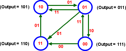
A simple example was chosen in order to acquaint the student with the type of design presented in this experiment. It does not necessarily correspond to anything practical, but was chosen for the simplicity needed to get the requisite familiarity. The state diagram of this system is shown in Figure 1.1. Each state is defined by the two bit WZ and each state produces an output defined by the three bits PQR. The inputs KL, needed to make the transitions between the states are indicated on the directed branches connecting the state balloons. It is implicit that when KL does not cause any transition that the system remains in the same state.
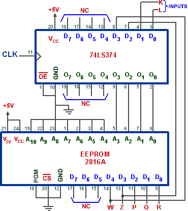
To gain familiarity with the use of EEPROMs, the two chip design of the type shown in Figure 1.2 was chosen.
The EEPROM contains the combinatorial logic and the octal D-type latch contains the needed bit storage. Both devices contain more logic than is needed for this design, so expansion should be possible. It is decided to pass the inputs FG through the latch, so that the system clock will control all the events and facilitates the testing of the system. The output bits PQR are derived combinatorially from the state bit WZ. Since the EEPROM has a substantial amount of unused logic we can put it to good use by using three of the EEPROM output lines for the output bits PQR. We determine the bit storage pattern for the EEPROM by creating a state table as shown in Table 1.1. Note that the present state and inputs supply the address to the EEPROM; the data outputs provide the next state and system outputs.
of Figure 1.1.
EPROMs or EEPROMs are useful for changeable designs. If you don’t like your first design, change it and reprogram the ROM. Rewiring is not required if your basic design is sound. We are using an EEPROM because it does not require a 20 minute erasure using a UV light device.
Before assembling a program, source code must be created with an editor or word processor (in ASCII mode). As an example, assume we are creating a source file for the state table in Figure 1.1, named TEST.ASM. A partial listing of directives for using the assembler ASM68K.EXE is given below:
ORG 0
DC.B $1E, $07, $07, $0B ; start assembling code from address 0
DC.B $0B, $1E, $07, $15 ; stores 4 bytes of date
DC.B $15, $0B, $15, $15
DC.B $1E, $15, $1E, $1E
END
Once the source file is edited it can be assembled using the assembler ASM68K.EXE. The assembler will produce a TEST.HEX files (S-records) which can then be used to program the EEPROM with the Superpro Programmer program.
| Table 1.1: The state table of the simple event-driven sequential circuit. | ||||||||
|---|---|---|---|---|---|---|---|---|
| Present State | Next State | |||||||
| State | Input | State | Output | |||||
| W | Z | F | G | W | Z | P | Q | R |
| 0 | 0 | 0 | 0 | 1 | 1 | 1 | 1 | 0 |
| 0 | 0 | 0 | 1 | 0 | 0 | 1 | 1 | 1 |
| 0 | 0 | 1 | 0 | 0 | 0 | 1 | 1 | 1 |
| 0 | 0 | 1 | 1 | 0 | 1 | 0 | 1 | 1 |
| 0 | 1 | 0 | 0 | 0 | 1 | 0 | 1 | 1 |
| 0 | 1 | 0 | 1 | 1 | 1 | 1 | 1 | 0 |
| 0 | 1 | 1 | 0 | 0 | 0 | 1 | 1 | 1 |
| 0 | 1 | 1 | 1 | 1 | 0 | 1 | 0 | 1 |
| 1 | 0 | 0 | 0 | 1 | 0 | 1 | 0 | 1 |
| 1 | 0 | 0 | 1 | 0 | 1 | 0 | 1 | 1 |
| 1 | 0 | 1 | 0 | 1 | 0 | 1 | 0 | 1 |
| 1 | 0 | 1 | 1 | 1 | 0 | 1 | 0 | 1 |
| 1 | 1 | 0 | 0 | 1 | 1 | 1 | 1 | 0 |
| 1 | 1 | 0 | 1 | 1 | 0 | 1 | 0 | 1 |
| 1 | 1 | 1 | 0 | 1 | 1 | 1 | 1 | 0 |
| 1 | 1 | 1 | 1 | 1 | 1 | 1 | 1 | 0 |
An Event Driven Annunciator System
The state diagram for the sequential circuit that we wish to design is shown in Figure 1.3. It is a two alarm system which might be used in factory to signal that various levels of faults are occurring on the production line. One application may be in process control, where the fault could indicate a high pressure. A flashing amber light would indicate the first state of pressure change, a potential hazard. A large change in the system, shown by a flashing red light would indicate an emergency condition.
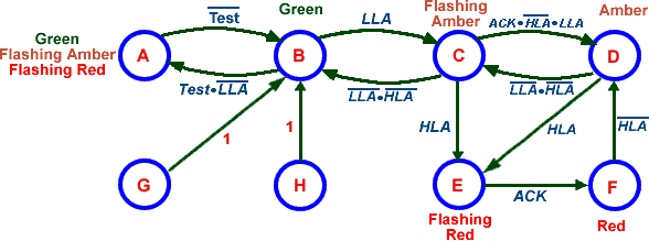
The annunciator has 6 proper states, so we shall need a 3 bit sequential circuit. Each state is described by the 3 bits UVW. For this example, states A through H have UVW = 000 to 111 respectively. The annunciator monitors the factory for the presence of a low-level alarm signal LLA and a high level alarm signal HLA. The high-level alarm signal HLA cannot occur if the low-level alarm signal LLA has not occurred first. The circuit operates in the following manner:
- With no fault signal present the system is stable, UVW equals 001 (B), and the GREEN light is on.
- When the signal LLA is present, indicating a minor fault, UVW changes to 010 (C), a FLASHING-AMBER light comes on and the GREEN light goes off. If the default disappears (LLA changes to 0), the annunciator returns directly to the normal GREEN state with UVW = 001 (B).
- If the system is in the minor fault (FLASHING-AMBER) state and an operator intervenes to clear the minor fault he pushes the acknowledge button which contains a momentary switch. The presence of the ACK signal of mere fraction of a second changes UVW to 011 (D) and the FLASHING-AMBER light becomes steady, telling supervisory personnel that someone is trying to clear the fault. If the minor fault is cleared (NOT LLA) the annunciator returns to the normal (GREEN) state by going to UVW = 010 (C) and if HLA is not present to UVW = 001 (B).
- If the system is in the AMBER or FLASHING-AMBER state and the major fault signal (HLA) is received, the system signals a major fault by changing UVW to 100 (E) which is the FLASHING-RED state. Even if this signal is only momentary, this condition will be maintained indefinitely. The presence of the ACK signal for a mere fraction of a second changes UVW to 101 (F) and the flashing red light becomes steady telling supervisory personnel that someone is trying to clear the major fault. If the major fault is cleared (NOT HLA), the annunciator starts on its path to the normal state by going to UVW = 011 (D) and continuing from there if LLA is also zero.
- A test pushbutton is included to check all the annunciator lights. On TEST, the GREEN, FLASHING-AMBER and FLASHING-RED lights should be on. The state is identified with UVW = 000 (A).
- In the event that one of the unused states (UVW = 110 or 111) (G or H) is erroneously entered, the system returns to the start state, UVW = 001 (B).
Prelab Assignment
Student should obtain their unique state sequences from the laboratory instructor. Each student should prepare a design similar to the one presented in this experiment which will realize the required state assignments for this design.
Laboratory Assignments
Program the EEPROM to realize the design of the annunciator for the required state assignments. Use the logic analyzer or a logic probe to debug the design and verify its operation to the laboratory instructor.